- 您现在的位置:买卖IC网 > Sheet目录312 > AT26DF081A-SSU (Atmel)IC FLASH 8MBIT 70MHZ 8SOIC
�� �
�
�7.� Read� Commands�
�7.1�
�Read� Array�
�The� Read� Array� command� can� be� used� to� sequentially� read� a� continuous� stream� of� data� from�
�the� device� by� simply� providing� the� SCK� signal� once� the� initial� starting� address� has� been� speci-�
�fied.� The� device� incorporates� an� internal� address� counter� that� automatically� increments� on� every�
�clock� cycle.�
�Two� opcodes,� 0Bh� and� 03h,� can� be� used� for� the� Read� Array� command.� The� use� of� each� opcode�
�depends� on� the� maximum� SCK� frequency� that� will� be� used� to� read� data� from� the� device.� The�
�0Bh� opcode� can� be� used� at� any� SCK� frequency� up� to� the� maximum� specified� by� f� SCK� .� The� 03h�
�opcode� can� be� used� for� lower� frequency� read� operations� up� to� the� maximum� specified� by� f� RDLF� .�
�To� perform� the� Read� Array� operation,� the� CS� pin� must� first� be� asserted� and� the� appropriate�
�opcode� (0Bh� or� 03h)� must� be� clocked� into� the� device.� After� the� opcode� has� been� clocked� in,� the�
�three� address� bytes� must� be� clocked� in� to� specify� the� starting� address� location� of� the� first� byte� to�
�read� within� the� memory� array.� If� the� 0Bh� opcode� is� used,� then� one� don't� care� byte� must� also� be�
�clocked� in� after� the� three� address� bytes.�
�After� the� three� address� bytes� (and� the� one� don't� care� byte� if� using� opcode� 0Bh)� have� been�
�clocked� in,� additional� clock� cycles� will� result� in� serial� data� being� output� on� the� SO� pin.� The� data�
�is� always� output� with� the� MSB� of� a� byte� first.� When� the� last� byte� (0FFFFFh)� of� the� memory� array�
�has� been� read,� the� device� will� continue� reading� back� at� the� beginning� of� the� array� (000000h).�
�No� delays� will� be� incurred� when� wrapping� around� from� the� end� of� the� array� to� the� beginning�
�of� the� array.�
�Deasserting� the� CS� pin� will� terminate� the� read� operation� and� put� the� SO� pin� into� a� high-imped-�
�ance� state.� The� CS� pin� can� be� deasserted� at� any� time� and� does� not� require� that� a� full� byte�
�of� data� be� read.�
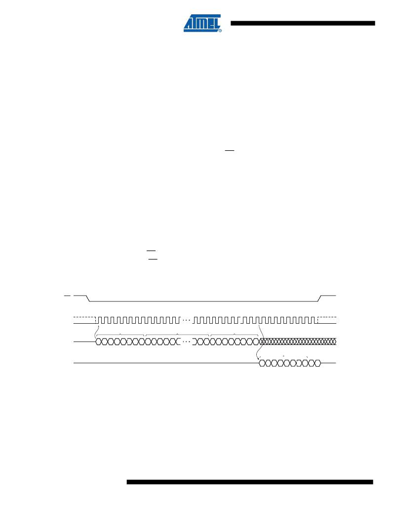
�Figure� 7-1.�
�Read� Array� –� 0Bh� Opcode�
�C� S�
�0�
�1�
�2�
�3�
�4�
�5�
�6�
�7�
�8�
�9�
�10� 11� 12�
�2� 9� 3� 0� 3� 1� 3� 2� 33� 3� 4� 3� 5� 3� 6� 3� 7� 38� 39� 40� 41� 42� 4� 3� 44� 45� 46� 47� 4� 8�
�S� CK�
�OPCODE�
�ADDRE� SS� BIT� S� A2� 3� -A0�
�DON'T� CARE�
�S� I�
�0�
�0�
�0�
�0�
�1�
�0�
�1�
�1�
�A�
�A�
�A�
�A�
�A�
�A�
�A�
�A�
�A�
�X�
�X�
�X�
�X�
�X�
�X�
�X�
�X�
�M� S� B�
�M� S� B�
�M� S� B�
�DATA� BYTE� 1�
�S� O�
�HIGH-IMPEDANCE�
�D�
�D�
�D�
�D�
�D�
�D�
�D�
�D�
�D�
�D�
�M� S� B�
�M� S� B�
�8�
�AT26DF081A�
�3600G–DFLASH–06/09�
�发布紧急采购,3分钟左右您将得到回复。
相关PDF资料
AT26DF161-SU
IC FLASH 16MBIT 66MHZ 8SOIC
AT26DF161A-MU
IC FLASH 16MBIT 70MHZ 8QFN
AT26DF321-SU
IC FLASH 32MBIT 66MHZ 8SOIC
AT27BV010-90JU
IC OTP 1MBIT 90NS 32PLCC
AT27BV020-90JU
IC OTP 2MBIT 90NS 32PLCC
AT27BV040-12JU
IC OTP 4MBIT 120NS 32PLCC
AT27BV1024-90JU
IC OTP 1MBIT 90NS 44PLCC
AT27BV256-70JU
IC OTP 256KBIT 70NS 32PLCC
相关代理商/技术参数
AT26DF081A-SSU-RET
制造商:Atmel Corporation 功能描述:
AT26DF081A-ST-B
制造商:Adesto Technologies Corporation 功能描述:8-SOIC-W, AUTO GRADE 3, 2.7V, TUBE - Rail/Tube
AT26DF081A-ST-T
制造商:Adesto Technologies Corporation 功能描述:8-SOIC-W, AUTO GRADE 3, 2.7V, T&R - Tape and Reel
AT26DF081A-SU
功能描述:闪存 8M 8 I/O Pins SPI 256B 2.7V-3.6V RoHS:否 制造商:ON Semiconductor 数据总线宽度:1 bit 存储类型:Flash 存储容量:2 MB 结构:256 K x 8 定时类型: 接口类型:SPI 访问时间: 电源电压-最大:3.6 V 电源电压-最小:2.3 V 最大工作电流:15 mA 工作温度:- 40 C to + 85 C 安装风格:SMD/SMT 封装 / 箱体: 封装:Reel
AT26DF081-MU
制造商:Adesto Technologies Corporation 功能描述:SF DATAFLASH, 8M, MLF, IND TEMP,GREEN - Trays
AT26DF081-SU
制造商:Adesto Technologies Corporation 功能描述:SF DATAFLASH, 8M, SOIC ,IND TEMP, GREEN - Rail/Tube
AT26DF161
制造商:ATMEL 制造商全称:ATMEL Corporation 功能描述:16-megabit 2.7-volt Only Serial Firmware DataFlash Memory
AT26DF161_06
制造商:ATMEL 制造商全称:ATMEL Corporation 功能描述:16-megabit 2.7-volt Only Serial Firmware DataFlash Memory